Technology
Accumulation of the know-how acquired from trial and error that Chichibu Denshi has experienced since its founding are leading to a unique and only one technology in the market. Introducing our technology.
- TOP
- Technology
INDEX
Commitment to Technology

Under the slogan of "pursuing the extreme quality of the surface," we have continued to innovate in order to meet the steadily increasing semiconductor miniaturization requests by the clients.
We are covering wide range of semiconductor materials from conventional silicon to silicon carbide, gallium nitride, which has been recently attracting attention as a material for next-generation power semiconductors, and lithium tantalate, which is expected for 5G. applications. We have been striving to provide the highest satisfaction for clients through various polishing services for a wide variety of materials.
The key the to polishing is how to polish it flat and how to clean it cleanly. We will continue to strive for technological development, keeping in mind that we will continue to be at the top in the industry as far as the flatness and the cleanliness are concerned.
Ever-Evolving Technological Development
Chichibu Denshi is constantly developing the following technologies.

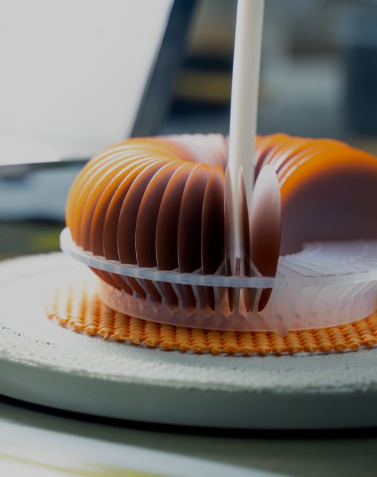
Polishing Technology with Extreme Flatness
Polishing is classified into DSP(double-sided polishing) which polishes both sides of the material, and SSP(single-sided polishing) which polishes only one side. Depending on the material, these two types of polishing are optimally applied to achieve the ultimate flatness.
In DSP, a flatness of 0.3μ or better is achieved with a 6inch substrate, and in SSP, a thickness tolerance of ± 0.1μ or better is achieved. These extreme flatness specifications enable the state of the art semiconductor minituarization.

Cutting Edge Cleaning Technology with Extreme Cleanleness
Most of the polished materials are processed in the pre-process of the clients semiconductor manufacturing. In order to avoid the heavy metal contamination, the cleanliness of the material surface after polishing is indispensable. We can respond flexibly to the heavy metal free request depending on the required heavy metal contamination level.
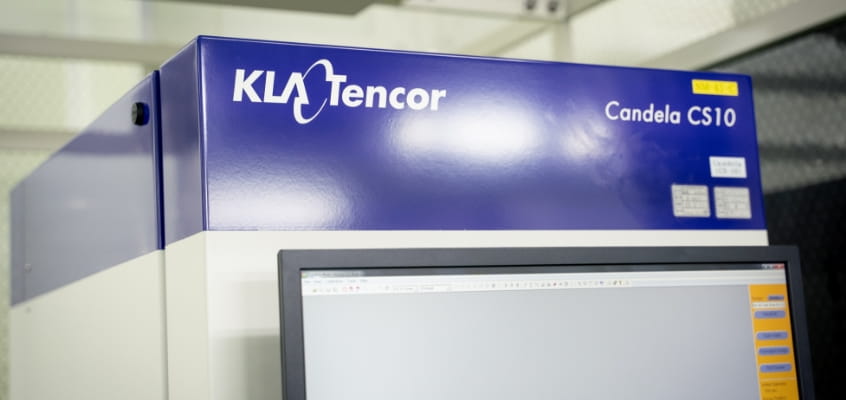
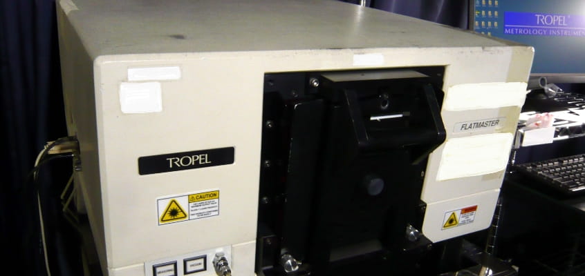
In addition, particles on the surface also affect significantly the yield of the pre-process, so the strict surface quality control is required. Our latest high precision inspection equipment can detect particles whose size is o.1μ or less. This inspection result can greatly contribute to the improvement of the pre-proccess yield.

High-Precision Special wafer processing technology
We can apply advanced special processing such as beveling (chamfering), laser marking, terrace processing (processing to make a step around the wafer), metal film vapor deposition, etc. to pre or after polished water depending on clients request. We can offer them as a one-stop service in combination with polishing.
Furthermore, as a business independent of polishing, we also provide an epitaxial growth processing service on silicon wafer.
Pursuit of Quality
ISO 9001 acquisition
We are coming out strict quality control under IS09001.
What is ISO 9001?
ISO 9001 is an international standard for quality management systems. It is the most popular management system standard and is used by more than 1 million organizations in more than 170 countries around the world.
IATF16949 certification
We have acquired IATF16949 certification and conduct strict quality control for the processing of in-vehicle products.
What is IATF?
IATF16949 is a quality management standard specific to the automotive industry and has been introduced by major automobile manufacturers around the world.
This standard is based on ISO9001 and has been adopted as a global procurement standard for automotive parts.
IATF 16949 defines the requirements for a quality management system and includes individual requirements specified by the customer.
Maintenance of Environment (ISO 14001 acquisition)
We are strictly monitoring and controlling the waste from the processing under ISO 14001.
We are contributing to the maintenance of the affluent nature in Chichibu area through ISO 14001.
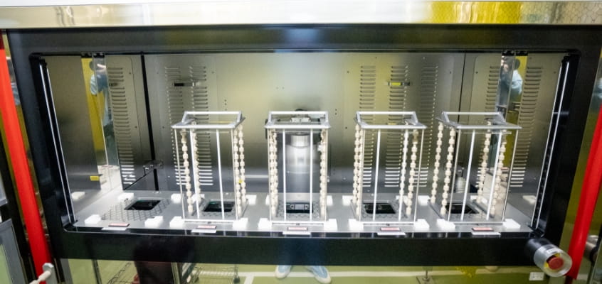
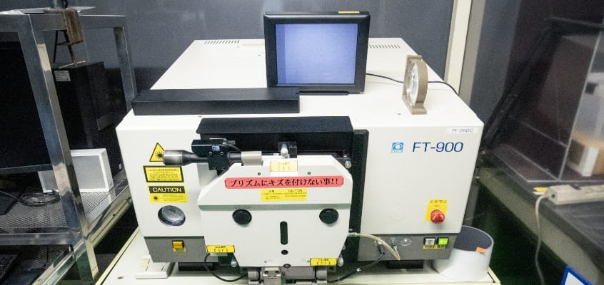
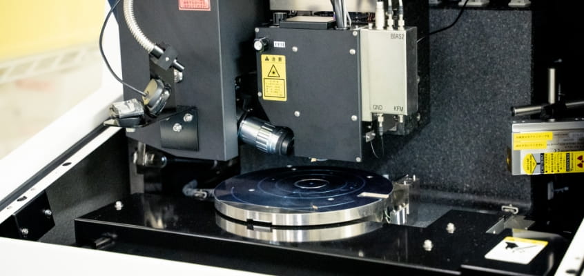
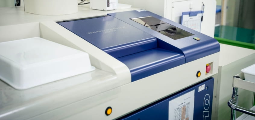
Installed Machine
Introducing the latest equipment installed at Chichibu Denshi.