Product & Processing
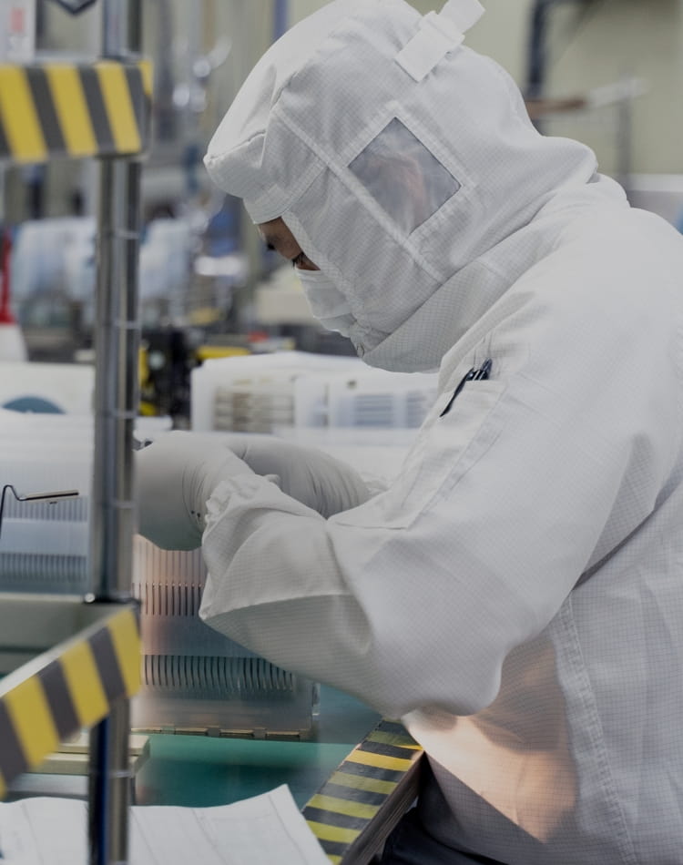
Chichibu Denshi is polishing various types of semiconductors.
In addition to this, it is also possible to make a prototype according to the client order.
- TOP
- Product & Processing
INDEX
Photomask Substrate Polishing Service
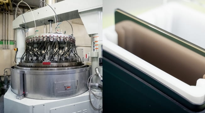
Polishing of synthetic quartz substrates used for semiconductor photomasks. We are focusing on recycling (re-polishing) used substrates. Our high yield of the remanufacturing is second to none. Our unique edge defect correction technology enables the high yield.
We are stripping chrome film on the surface of the used substrate by our environment-friendly chrome film peeling process. After the stripping, the substrated are put into the polishing process. Furthermore, the device pattern drawn on the surface is a trade secret. Thus, the substrattes with the chrome film are stored under the highest security by strict entrance control.
AS for a 6-inch substrate, the flatness of the polished surface is 0.3μ or better and the counts of 0.1μ size particle is almost"0".
Special Wafer Polishing Service for the Next-generation Power Semiconductors
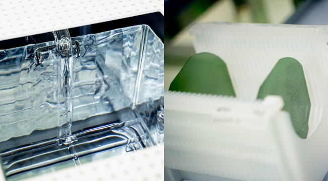
We are polishing silicon carbide (SiC) and gallium nitride (GaN) wafers. These materials are very promissing with high efficiency in switching(low switchingless) and are expected to greatly contribute to the improvement of cruising range of electric vehicles or hybrid cars.
We are offering various polishing services such as epi remoral backside polishing after epigrowth, backside polishing after device making proccess and recycle polishing of the used wafer, etc. In addition, we can also perform additional processing such as beveling, laser marking,etc, upon client's request.
Heavy metal-free cleanliness is required the surface for the polished wafers because they are processed in the pre-process of the semiconductor manufacturing.TXRF is installed in-house to assure heavy metal-free polished surface.
Epitaxy Growth Service
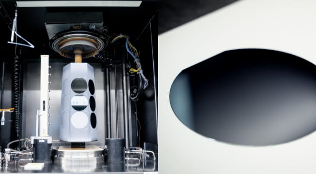
We are offering epitaxy growth services on 4, 5 and 6 inch silicon wafers. Efficient production is carried out by our batch type epi equipment. Our clients are satisfied with the short delivery time and the reasonable processing price. A diffusion furnace is also installed in the process, and it is possible to provide diffusion processing services in combination with epi-growth.
SAW Filter Wafer Polishing Service
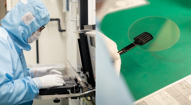
Lithium tantalate wafer polishing service for SAW filters for 5G, whose demand will increase dramatically in the near future. SAW filter is a semiconductor that filters signal frequencies using surface acoustic waves. Due to this, extremely fine flatness on the polished surface is indispensable. We can the realize thickness tolerance of ± 0.1μ through our cutting edge polishing machines. This accuracy has been highly evaluated by our clients.
At the same time, we can offer terrace processing service around the wafer (processing to make a step on the end surface of the wafer). The combination of the wafer polishing and the terrace processing service is unique and highly evaluated in the market.
Silicon Wafer Back Side Polishing Service
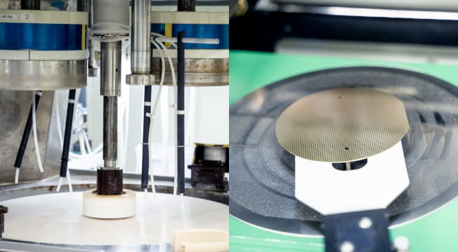
For silicon wafers with devices pattern on the front surface, we polish the back side by protecting the front device surface. The processing size is 4 to 12inch, and the finishing thickness can be up to about 50μ. Our water standard finish is grinding with fixed abrasive grains.
If necessary, polishing with free abrasive grains is possible after the grinding. If in a hurry, we can handle it for 2 days and 1 night (deliver the day after the receipt). A small amount processing is also possible. We are respond flexibly to customer's requests.
Compound Semiconductor Wafer Polishing Service
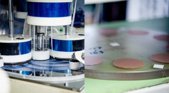
Applications of compound semiconductor wafers are wide-ranging such as high-frequency devices, laser oscillation devices, LEDs ,etc. We are polishing various types of compound semiconductor wafers such as gallium phosphide (GaP), gallium arsenide (GaAs), indium phosphide (InP), etc.
Various processings such as grinding, wrapping, polishing, etc are optimally combined to meet customer's wide ranging needs such as substrate polishing, recycling polishing, backside polishing, etc. Some compound semiconductor wafers are not flat in shape and sometimes are greatly warped. Our processing know-how to correct the warp is second to none and enables the polishing of these irregular surfaces shape wafers.
Metal Film Vapor Deposition Service
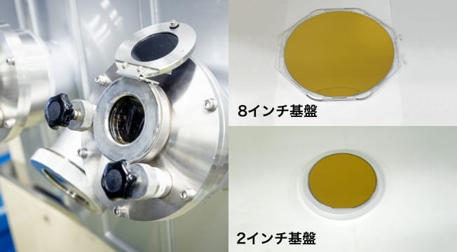
We are ofering metal film deposition service on the back surface of the polished silicon or compound semiconductor wafer. we are unique in doing the metal film deposition and the polishing simultaneously as an one-stop service. We are covering a wide variety of metal films such as Au, Pt, Al, Cu, etc.
